作者中心
作者中心 专家审稿
专家审稿 责编办公
责编办公 编辑办公
编辑办公
-
摘要: 微波光子集成芯片技术是微波光子雷达的重要支撑技术,不仅可以实现器件的多功能化,缩小微波光子雷达的体积,还可以大大提升微波光子雷达的稳定性与可靠性。该文介绍了目前常用的InP基、Si基和铌酸锂基等材料体系及其异质异构集成的光子集成芯片技术和可用于微波光子混合集成的光电集成芯片技术,并展望了未来发展趋势。Abstract: Microwave photonic integrated chip technology is an important supporting technology of microwave photonic radar. It can not only realize the multifunction of devices, reduce the volume of microwave photonic radar, but also greatly improve the stability and reliability. This paper introduces the photonic integrated chip technologies based on the commonly used InP, Si, LiNbO3 and their heterogeneous integrations and the optoelectronic integration chip technologies for microwave photonics. Finally, the future development trends is discussed.
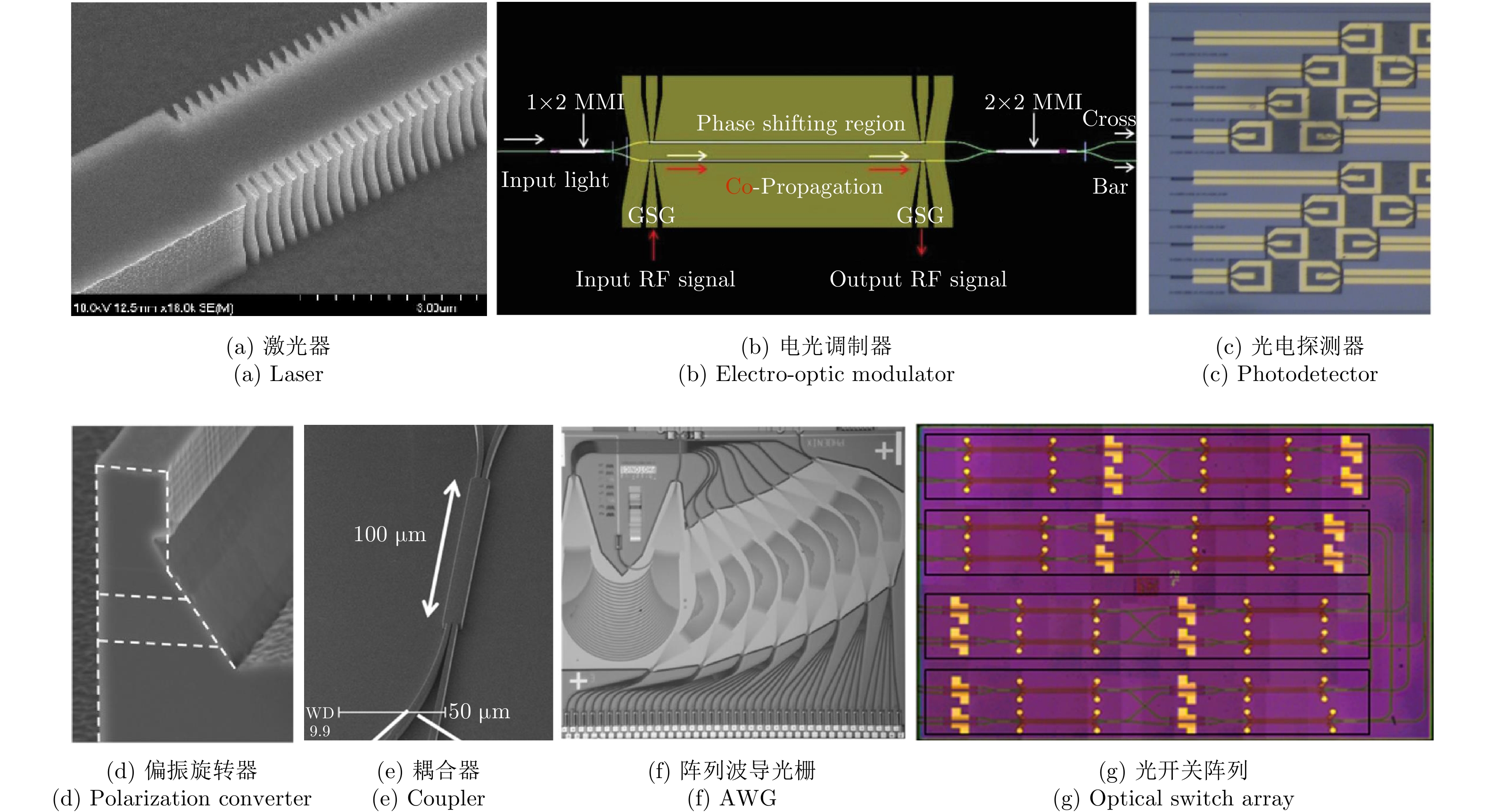
-

表 1 报道的一些集成光子器件及性能
Table 1. Some reported integrated photonic devices and their performances
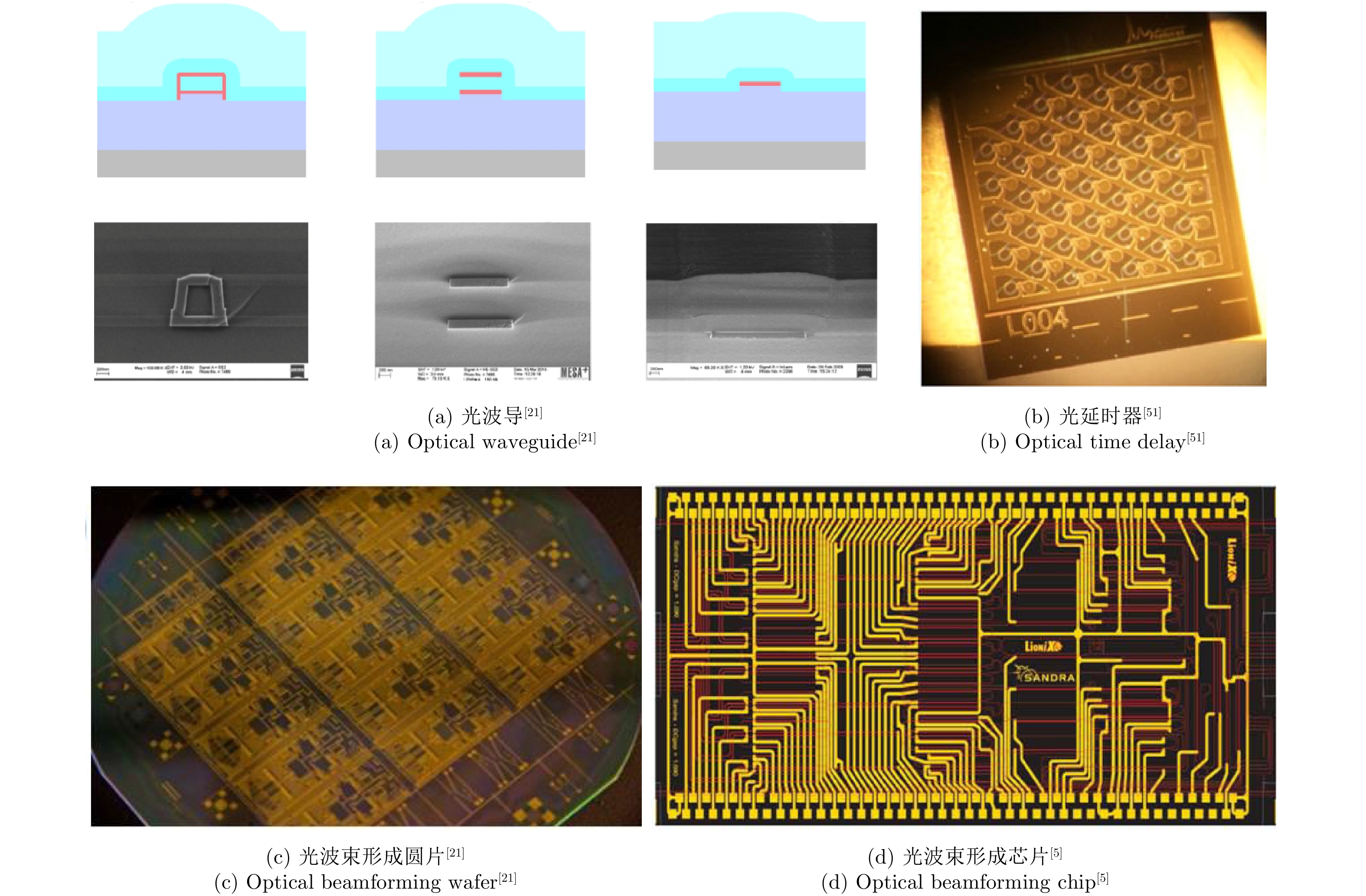
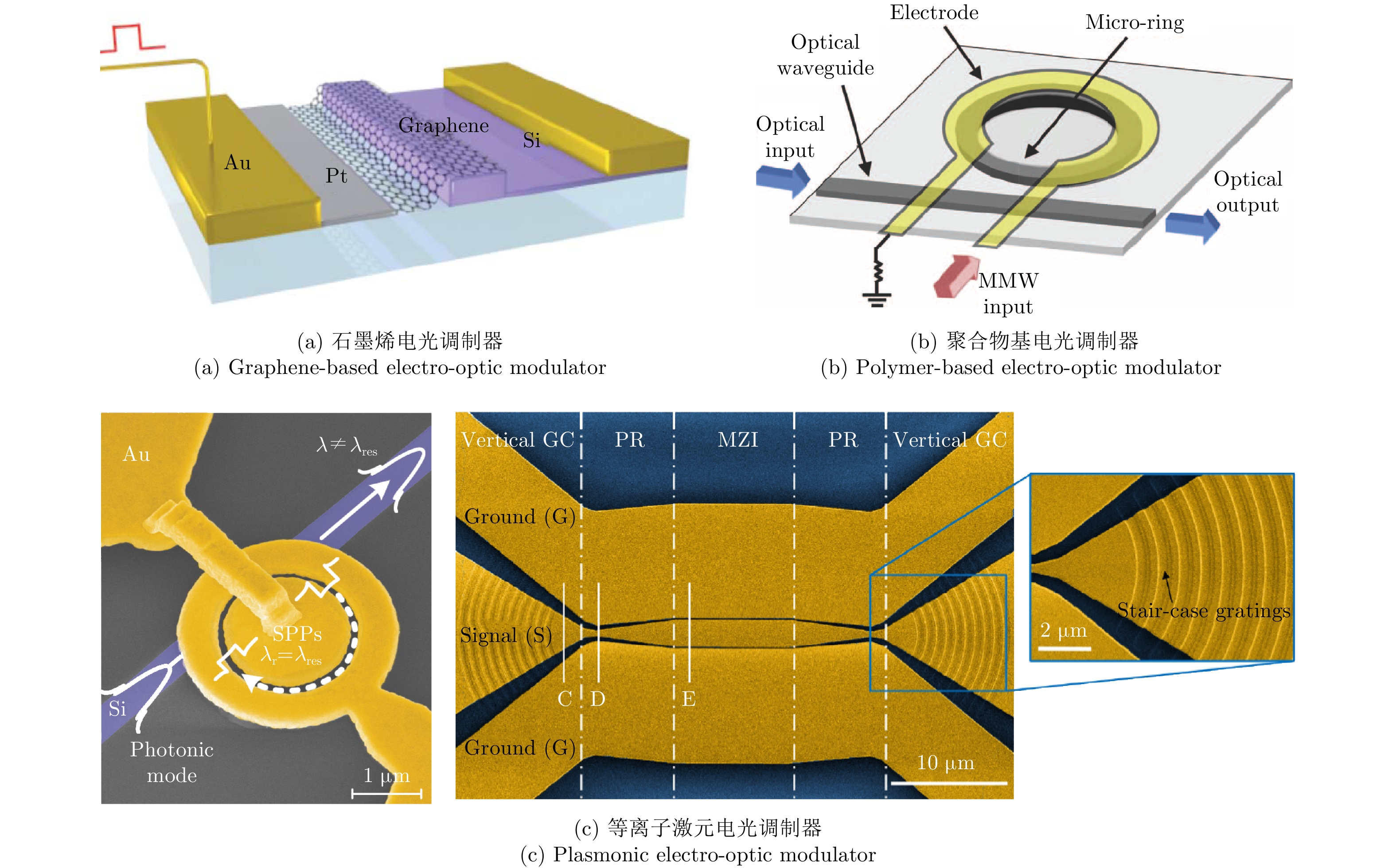
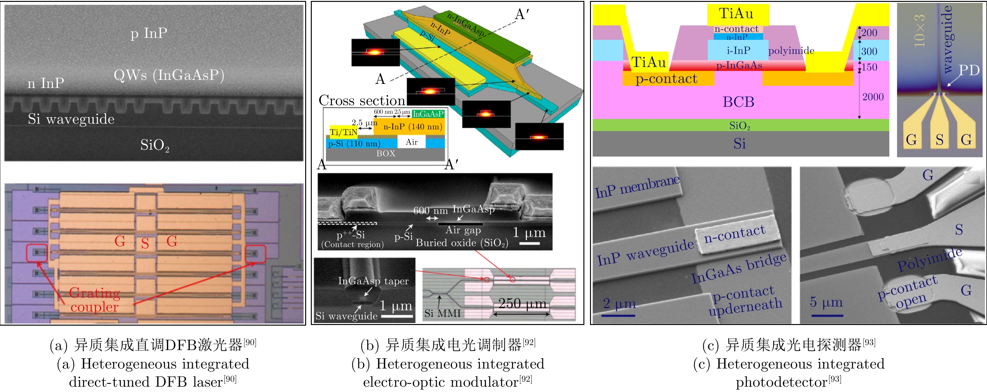
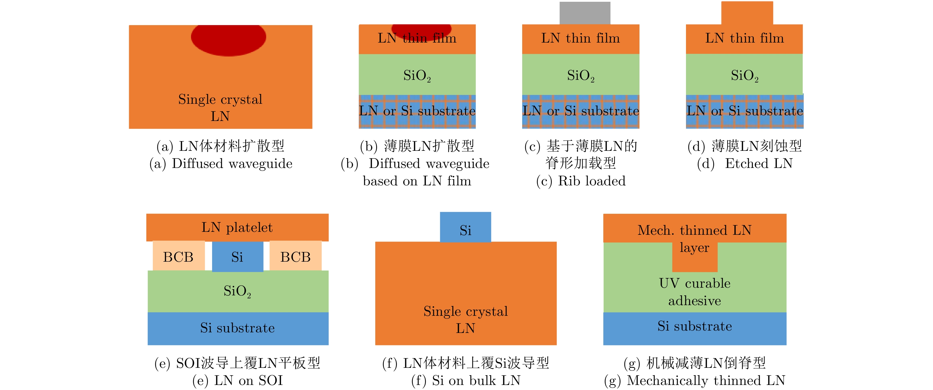
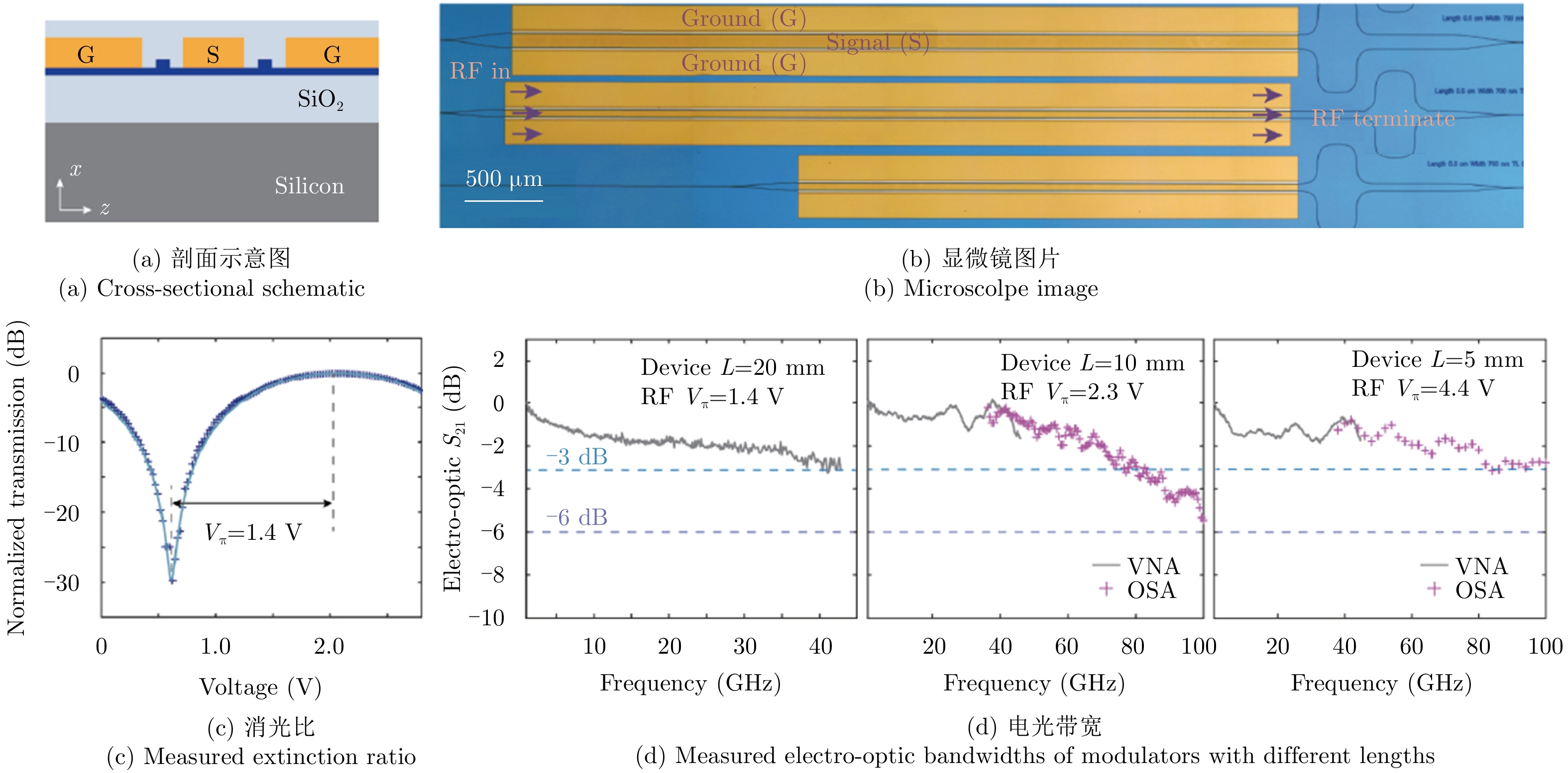
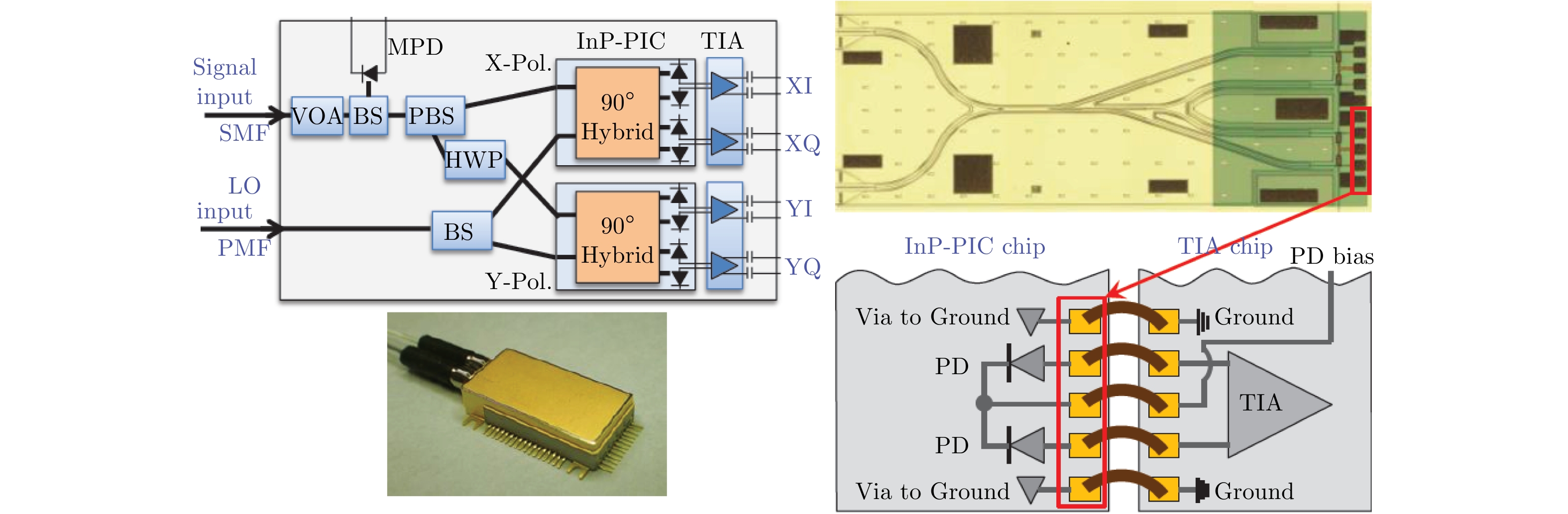
材料 时间 第一作者国籍 器件 指标 InP 1999 The Netherlands 波束形成[105] 通道:1×16,插损:28±1.0 dB,相位动态范围:360° 2004 Germany 波导型PD[106] 带宽:100 GHz,响应度:0.66 A/W 2010 USA OPLL[107] 带宽:300 MHz 2011 USA 可编程微波光子滤波器[108] 带宽:1.9~14 GHz, SFDR: 86.3 dB×Hz2/3 2013 China DFB激光器阵列[109] 通道数:4 2014 Germany 平衡PD[110] 带宽:80 GHz,响应度:0.5 A/W 2016 Germany DFB+IQ电光调制器[111] 带宽:43 GHz,耦合损耗:0.1 dB 2017 Sweden 外调制激光器[112] 带宽:100 GHz,消光比:~30 dB 2017 Japan IQ调制器[113] 带宽:>67 GHz,半波电压:1.5 V,消光比:~30 dB 2017 China AWG+PD[114] 响应度:0.68 A/W,带宽:>16 GHz,通道数:13 2017 Germany 波导型PD[115] 带宽:80 GHz,响应度:0.5 A/W 2017 Germany 波导型平衡PD[116] 带宽:115 GHz,响应度:0.25 A/W 2018 UK 开关阵列[10] 规模:4×4,串扰:–47 dB Si 2004 USA 调制器[29] 带宽:1 GHz,调制效率:8 V·cm,插损:15.3 dB,静态消光比:16 dB 2005 USA 拉曼激光器[23] 波长:1.67 μm,线宽:80 MHz,边模抑制比:55 dB 2007 USA 调制器[30] 带宽:30 GHz,速率:40 Gbit/s,动态消光比:1.1 dB 2007 USA GeSi探测器[36] 带宽:31 GHz,响应度:0.89 A/W,暗电流:169 nA 2009 USA GeSi探测器[37] 带宽:36.8 GHz,响应度:1.1 A/W 2011 China 延时线[47] 延时量:–15~85 ps 2012 USA GeSi激光器[26] 波长:1520~1700 nm,线宽:<1.2 nm,输出功率:>1 mW 2012 UK 调制器[31] 消光比:3.1 dB,调制效率:2.8 V·cm,带宽:20 GHz 2012 China 调制器[32] 消光比:3.9 dB@40 Gbit/s,调制效率:2.6 V·cm 2012 China 延时线[48] 延时量:270 ps, FWHM=2.1 GHz 2013 Australia 微波带阻滤波器[50] FWHM=247~840 MHz,抑制比:60 dB,中心频率范围:2~8 GHz 2013 Singapore 调制器[33] 消光比:5.56 dB,调制效率:26.7 V·mm,带宽:25.6 GHz 2013 China 微波带阻滤波器[44] 10 dB带宽:1.85~4.55 GHz,中心频率调谐范围:7~34 GHz 2013 The Netherlands 波束形成网络[52] 规模:1×4,最大延时:236 ps,工作频率:10.70~12.75 GHz 2016 China 开关阵列[45] 规模:16×16,串扰:–30 dB,开关时间:22 μm,插损:5.2 dB 2017 Japan 调制器[34] 带宽:17 GHz,调制效率:0.8~1.86 V·cm 2017 Canada 集成微波带通滤波器[42] FWHM=2.3 GHz,抑制比:17 dB,中心频率调谐范围:7~25 GHz 2017 USA 波束形成网络[53] 规模:1×4,带宽:6 GHz,最大延时:209 ps 2018 China 调制器[35] 带宽:60 GHz,速率:100 Gbit/s,调制效率1.4 V·cm,插损:5.4 dB 2018 China GeSi探测器[40] 带宽:25 GHz,响应度:0.88 A/W 2018 Canada 集成OEO[41] 相噪:–80 dBc/Hz,频率:2~8 GHz 2018 China 微波带通滤波器[43] FWHM=170 MHz,抑制比:26.5 dB,中心频率调谐范围:2.0~18.4 GHz 2018 USA 真延时[51] 损耗:0.89 dB/ns,延时量调谐范围:0~3.4 ns,带宽:10 GHz@500 ps LiNbO3 1998 Israel 调制器[117] 带宽:40 GHz,半波电压:4.2 V 2007 Switzerland 可调谐谐振腔[118] R=100 μm, Q=4×10³,清晰度F=5 2009 USA 调制器[65] 带宽:~100 GHz,半波电压:7 V,插损:3.7 dB 2010 China 1×2 Y分支光开关[119] 串扰:–30 dB Polymer 1997 USA 调制器[81] 带宽:113 GHz 2002 USA 环形滤波器、调制器[76] Q=1.3×10⁵,谐振调谐效率:0.82 GHz/V 2015 China 开关阵列[120] 规模:1×32 2016 China 调制器[121] 电光系数:50 pm/V,半波电压:1.94 V SPP 2010 Denmark 热光开关[122] 器件长度:<100 μm 2015 Switzerland 天线+调制器 工作频率:60 GHz,转换效率:–25 dB 2017 Switzerland 调制器[83] 器件长度:几十μm,带宽:>70 GHz 2018 Switzerland 环形调制器[123] R=1 μm, Q=30, FSR≈115 nm Graphe 2011 USA 调制器[68] 光带宽:1.35~1.6 μm 2013 Turkey 调制器[124] 光带宽:450 nm~2 μm 2015 UK 调制器[125] 调制深度:>0.03 dB/μm Si-InP 2016 Belgium 激光器[90] 波长:1566 nm,边模抑制比:45 dB,波导输出光功率:6 mW,直调带宽:15 GHz 2016 USA 探测器[126] 响应度:0.64 A/W,输出功率:12 dBm@40 GHz,带宽:48 GHz 2016 The Netherlands 波导型探测器 带宽:67 GHz,响应度:0.7 A/W 2017 Japan 调制器[92] 带宽:2.2 GHz,调制效率:0.09 V·cm,消光比:3.1 dB@32 Gbit/s 2018 Belgium 外调制激光器[127] 波长:1567 nm,边模抑制比:40 dB,波导输出光功率:3 mW,带宽:20 GHz,静态消光比:15 dB Si-LiNbO3 2014 USA 环形调制器[128] 带宽:5 GHz, Q值:14000,谐振调谐效率:3.3 pm/V 2016 USA 调制器[67] 带宽:>8 GHz,半波电压:2.5 V,消光比:13.8 dB 2016 USA 调制器[96] 带宽:~40 GHz 2018 USA 调制器[97] 带宽:100 GHz,半波电压:5 V,消光比:~30 dB 2019 China 调制器[98] 带宽:>70 GHz,半波电压:<7.4 V,消光比:~40 dB,插损:2.5 dB 2019 USA 电光可调谐光频梳[129] 调谐范围:10~100 MHz  下载: 导出CSV
-
[1] CAPMANY J and NOVAK D. Microwave photonics combines two worlds[J]. Nature Photonics, 2007, 1(6): 319–330. doi: 10.1038/nphoton.2007.89 [2] 潘时龙, 张亚梅. 微波光子雷达及关键技术[J]. 科技导报, 2017, 35(20): 36–52.PAN Shilong and ZHANG Yamei. Microwave photonic radar and key technologies[J]. Science &Technology Review, 2017, 35(20): 36–52. [3] GHELFI P, LAGHEZZA F, SCOTTI F, et al. A fully photonics-based coherent radar system[J]. Nature, 2014, 507(7492): 341–345. doi: 10.1038/nature13078 [4] CAPMANY J, LI Guifang, LIM C, et al. Microwave photonics: Current challenges towards widespread application[J]. Optics Express, 2013, 21(19): 22862–22867. doi: 10.1364/OE.21.022862 [5] MARPAUNG D, ROELOFFZEN C, HEIDEMAN R, et al. Integrated microwave photonics[J]. Laser & Photonics Reviews, 2013, 7(4): 506–538. doi: 10.1002/lpor.201200032 [6] MUÑOZ P, CAPMANY J, PÉREZ D, et al. Integrated microwave photonics: State of the art and future trends[C]. Proceedings of the 16th International Conference on Transparent Optical Networks (ICTON), Graz, Austria, 2014: 1–4. doi: 10.1109/ICTON.2014.6876725. [7] HOU Lianping, HAJI M, AKBAR J, et al. AlGaInAs/InP monolithically integrated DFB laser array[J]. IEEE Journal of Quantum Electronics, 2012, 48(2): 137–143. doi: 10.1109/JQE.2011.2174455 [8] SADIQ M U, ROYCROFT B, O’CALLAGHAN J, et al. Efficient modelling approach for an InP based Mach-Zehnder modulator[C]. Proceedings of the 25th IET Irish Signals & Systems Conference 2014 and 2014 China-Ireland International Conference on Information and Communications Technologies, Limerick, Ireland, 2014. doi: 10.1049/cp.2014.0671. [9] AUGUSTIN L M, HANFOUG R, VAN DER TOL J J G M, et al. A compact integrated polarization splitter/converter in InGaAsP-InP[J]. IEEE Photonics Technology Letters, 2007, 19(17): 1286–1288. doi: 10.1109/LPT.2007.902277 [10] DING Minsheng, WONFOR A, Cheng Qixiang, et al. Hybrid MZI-SOA InGaAs/InP photonic integrated switches[J]. IEEE Journal of Selected Topics in Quantum Electronics, 2018, 24(1): 3600108. doi: 10.1109/JSTQE.2017.2759278 [11] SMIT M, LEIJTENS X, AMBROSIUS H, et al. An introduction to InP-based generic integration technology[J]. Semiconductor Science and Technology, 2014, 29(8): 083001. doi: 10.1088/0268-1242/29/8/083001 [12] VAN DER TOL J J G M, OEI Y S, KHALIQUE U, et al. InP-based photonic circuits: Comparison of monolithic integration techniques[J]. Progress in Quantum Electronics, 2010, 34(4): 135–172. doi: 10.1016/j.pquantelec.2010.02.001 [13] WU Fang, TOLSTIKHIN V I, DENSMORE A S, et al. Two-step lateral taper spot-size converter for efficient fiber coupling to InP-based photonic integrated circuits[C]. Proceedings Volume 5577, Photonics North 2004: Optical Components and Devices, Ottawa, Ontario, Canada, 2004: 213–220. doi: 10.1117/12.567349. [14] KOHTOKU M, OKU S, KADOTA Y, et al. Spotsize converter with improved design for InP-based deep-ridge waveguide structure[J]. Journal of Lightwave Technology, 2005, 23(12): 4207–4214. doi: 10.1109/JLT.2005.854042 [15] KITAMURA T, KONO N, YAGI H, et al. Dual-core spot-size converter with tapered cladding layer designed for high-efficiency mode coupling to InP-based deep-ridge waveguide[C]. Proceedings of 2014 IEEE Photonics Conference, San Diego, USA, 2014: 280–281. doi: 10.1109/IPCon.2014.6995353. [16] SOARES F M, KAROUTA F, GELUK E J, et al. A compact and fast photonic true-time-delay beamformer with integrated spot-size converters[C]. Proceedings of Integrated Photonics Research and Applications/Nanophotonics, Uncasville, Connecticut United States, 2006. doi: 10.1364/IPRA.2006.IMF5. [17] KIM D J, HAN W S, KIM D Y, et al. InP-based vertical dual-waveguide fiber-coupling structure[C]. Proceedings of the 12th International Conference on Optical Internet, Jeju, South Korea, 2014: 1–2. doi: 10.1109/COIN.2014.6950599. [18] TOLSTIKHIN V, SAEIDI S, and DOLGALEVA K. Design optimization and tolerance analysis of a spot-size converter for the taper-assisted vertical integration platform in InP[J]. Applied Optics, 2018, 57(13): 3586–3591. doi: 10.1364/AO.57.003586 [19] WON R and PANICCIA M. Integrating silicon photonics[J]. Nature Photonics, 2010, 4(8): 498–499. doi: 10.1038/nphoton.2010.189 [20] ZHUANG Leimeng, MARPAUNG D, BURLA M, et al. Low-loss, high-index-contrast Si3N4/SiO2 optical waveguides for optical delay lines in microwave photonics signal processing[J]. Optics Express, 2011, 19(23): 23162–23170. doi: 10.1364/OE.19.023162 [21] ROELOFFZEN C G H, ZHUANG Leimeng, TADDEI C, et al. Silicon nitride microwave photonic circuits[J]. Optics Express, 2013, 21(19): 22937–22961. doi: 10.1364/OE.21.022937 [22] SOREF R. The past, present, and future of silicon photonics[J]. IEEE Journal of Selected Topics in Quantum Electronics, 2006, 12(6): 1678–1687. doi: 10.1109/JSTQE.2006.883151 [23] RONG Haisheng, JONES R, LIU Ansheng, et al. A continuous-wave Raman silicon laser[J]. Nature, 2005, 433(7027): 725–728. doi: 10.1038/nature03346 [24] LIU Jifeng, SUN Xiaochen, PAN Dong, et al. Tensile-strained, n-type Ge as a gain medium for monolithic laser integration on Si[J]. Optics Express, 2007, 15(18): 11272–11277. doi: 10.1364/OE.15.011272 [25] LIU Jifeng, SUN Xiaochen, CAMACHO-AGUILERA R, et al. Ge-on-Si laser operating at room temperature[J]. Optics Letters, 2010, 35(5): 679–681. doi: 10.1364/OL.35.000679 [26] CAMACHO-AGUILERA R E, CAI Yan, PATEL N, et al. An electrically pumped germanium laser[J]. Optics Express, 2012, 20(10): 11316–11320. doi: 10.1364/OE.20.011316 [27] LIU Jifeng, KIMERLING L C, and MICHEL J. Monolithic Ge-on-Si lasers for large-scale electronic-photonic integration[J]. Semiconductor Science and Technology, 2012, 27(9): 094006. doi: 10.1088/0268-1242/27/9/094006 [28] DUTT B, SUKHDEO D S, NAM D, et al. Roadmap to an efficient germanium-on-silicon laser: Strain vs. n-type doping[J]. IEEE Photonics Journal, 2012, 4(5): 2002–2009. doi: 10.1109/jphot.2012.2221692 [29] LIU Ansheng, JONES R, LIAO L, et al. A high-speed silicon optical modulator based on a metal-oxide-semiconductor capacitor[J]. Nature, 2004, 427(6975): 615–618. doi: 10.1038/nature02310 [30] LIAO L, LIU A, RUBIN D, et al. 40 Gbit/s silicon optical modulator for highspeed applications[J]. Electronics Letters, 2007, 43(22): 9944669. doi: 10.1049/el:20072253 [31] THOMSON D J, GARDES F Y, FEDELI J M, et al. 50-Gb/s silicon optical modulator[J]. IEEE Photonics Technology Letters, 2012, 24(4): 234–236. doi: 10.1109/LPT.2011.2177081 [32] HU Yingtao, XIAO Xi, XU Hao, et al. High-speed silicon modulator based on cascaded microring resonators[J]. Optics Express, 2012, 20(14): 15079–15085. doi: 10.1364/oe.20.015079 [33] TU Xiaoguang, LIOW T Y, SONG Junfeng, et al. 50-Gb/s silicon optical modulator with traveling-wave electrodes[J]. Optics Express, 2013, 21(10): 12776–12782. doi: 10.1364/OE.21.012776 [34] MAEGAMI Y, CONG Guangwei, OHNO M, et al. High-efficiency strip-loaded waveguide based silicon Mach-Zehnder modulator with vertical p-n junction phase shifter[J]. Optics Express, 2017, 25(25): 31407–31416. doi: 10.1364/oe.25.031407 [35] LI Miaofeng, WANG Lei, LI Xiang, et al. Silicon intensity Mach-Zehnder modulator for single lane 100 Gb/s applications[J]. Photonics Research, 2018, 6(2): 109–116. doi: 10.1364/prj.6.000109 [36] YIN Tao, COHEN R, MORSE M M, et al. 31GHz Ge n-i-p waveguide photodetectors on silicon-on-insulator substrate[J]. Optics Express, 2007, 15(21): 13965–13971. doi: 10.1364/OE.15.013965 [37] FENG Dazeng, LIAO Shirong, DONG Po, et al. High-speed Ge photodetector monolithically integrated with large cross-section silicon-on-insulator waveguide[J]. Applied Physics Letters, 2009, 95(26): 261105. doi: 10.1063/1.3279129 [38] MICHEL J, LIU Jifeng, and KIMERLING L C. High-performance Ge-on-Si photodetectors[J]. Nature Photonics, 2010, 4(8): 527–534. doi: 10.1038/nphoton.2010.157 [39] LIAO Shirong, FENG Ningning, FENG Dazeng, et al. 36 GHz submicron silicon waveguide germanium photodetector[J]. Optics Express, 2011, 19(11): 10967–10972. doi: 10.1364/OE.19.010967 [40] CUI Jishi, BAI Bowen, YANG Fenghe, et al. Optical saturation characteristics of dual- and single-injection Ge-on-Si photodetectors[J]. Chinese Optics Letters, 2018, 16(7): 072502. [41] ZHANG Weifeng and YAO Jianping. Silicon photonic integrated optoelectronic oscillator for frequency-tunable microwave generation[J]. Journal of Lightwave Technology, 2018, 36(19): 4655–4663. doi: 10.1109/JLT.2018.2829823 [42] ZHANG Weifeng and YAO Jianping. On-chip silicon photonic integrated frequency-tunable bandpass microwave photonic filter[J]. Optics Letters, 2018, 43(15): 3622–3625. doi: 10.1364/OL.43.003622 [43] QIU Huaqing, ZHOU Feng, QIE Jinran, et al. A continuously tunable sub-gigahertz microwave photonic bandpass filter based on an ultra-high-Q silicon microring resonator[J]. Journal of Lightwave Technology, 2018, 36(19): 4312–4318. doi: 10.1109/JLT.2018.2822829 [44] ZHANG Dengke, FENG Xue, LI Xiangdong, et al. Tunable and reconfigurable bandstop microwave photonic filter based on integrated microrings and Mach-Zehnder interferometer[J]. Journal of Lightwave Technology, 2013, 31(23): 3668–3675. doi: 10.1109/jlt.2013.2287091 [45] ZHAO Shuoyi, LU Liangjun, ZHOU Linjie, et al. 16×16 silicon Mach-Zehnder interferometer switch actuated with waveguide microheaters[J]. Photonics Research, 2016, 4(5): 202–207. doi: 10.1364/PRJ.4.000202 [46] TESTA F, OTON C J, KOPP C, et al. Design and implementation of an integrated reconfigurable silicon photonics switch matrix in IRIS project[J]. IEEE Journal of Selected Topics in Quantum Electronics, 2016, 22(6): 155–168. doi: 10.1109/JSTQE.2016.2547322 [47] HU Yingtao, XIAO Xi, LI Xianyao, et al. Continuously tunable time delay and advance in coupling-modulated microring resonators[C]. Proceedings of SPIE 8333, Photonics and Optoelectronics Meetings 2011: Optoelectronic Devices and Integration, Wuhan, China, 2011: 833303. doi: 10.1117/12.920404. [48] ZHOU L, SUN X, XIE J, et al. Characterisation of microring resonator optical delay and its dependence on coupling gap using modulation phase-shift technique[J]. Electronics Letters, 2012, 48(25): 1613–1614. doi: 10.1049/el.2012.2743 [49] WANG Junjia, ASHRAFI R, ADAMS R, et al. Subwavelength grating enabled on-chip ultra-compact optical true time delay line[J]. Scientific Reports, 2016, 6: 30235. doi: 10.1038/srep30235 [50] MARPAUNG D, MORRISON B, PANT R, et al. Si3N4 ring resonator-based microwave photonic notch filter with an ultrahigh peak rejection[J]. Optics Express, 2013, 21(20): 23286–23294. doi: 10.1364/OE.21.023286 [51] XIANG Chao, DAVENPORT M L, KHURGIN J B, et al. Low-loss continuously tunable optical true time delay based on si3n4 ring resonators[J]. IEEE Journal of Selected Topics in Quantum Electronics, 2018, 24(4): 5900109. doi: 10.1109/JSTQE.2017.2785962 [52] BURLA M, MARPAUNG D, ZHUANG Leimeng, et al. Integrated photonic Ku-band beamformer chip with continuous amplitude and delay control[J]. IEEE Photonics Technology Letters, 2013, 25(12): 1145–1148. doi: 10.1109/LPT.2013.2257723 [53] LIU Yuan, WICHMAN A, ISAAC B, et al. Tuning optimization of ring resonator delays for integrated optical beam forming networks[J]. Journal of Lightwave Technology, 2017, 35(22): 4954–4960. doi: 10.1109/JLT.2017.2762641 [54] KAMINOW I P, CARRUTHERS J R, TURNER E H, et al. Thin-film LiNbO3 electro-optic light modulator[J]. Applied Physics Letters, 1973, 22(10): 540–542. doi: 10.1063/1.1654500 [55] HOWERTON M M, MOELLER R P, GREENBLATT A S, et al. Fully packaged, broad-band LiNbO3 modulator with low drive voltage[J]. IEEE Photonics Technology Letters, 2000, 12(7): 792–794. doi: 10.1109/68.853502 [56] DOLFI D W and RANGANATH T R. 50 GHz velocity-matched broad wavelength LiNbO3 modulator with multimode active section[J]. Electronics Letters, 1992, 28(13): 1197–1198. doi: 10.1049/el:19920756 [57] IZUTSU M, YAMANE Y, and SUETA T. Broad-band traveling-wave modulator using a LiNbO3 optical waveguide[J]. IEEE Journal of Quantum Electronics, 1977, 13(4): 287–290. doi: 10.1109/JQE.1977.1069310 [58] KAWANISHI T, SAKAMOTO T, TSUCHIYA M, et al. 70dB extinction-ratio LiNbO3 optical intensity modulator for two-tone lightwave generation[C]. Proceedings of Optical Fiber Communication Conference and Exposition and The National Fiber Optic Engineers Conference, Anaheim, California, USA, 2006: 1–3. doi: 10.1109/OFC.2006.215457. [59] KONDO J, AOKI K, IWATA Y, et al. 76-GHz millimeter-wave generation using MZ LiNbO3 modulator with drive voltage of 7 Vp-pand 19 GHz signal input[C]. Proceedings of 2005 International Topical Meeting on Microwave Photonics, Seoul, Korea, 2005. doi: 10.1109/MWP.2005.203613. [60] SAKAMOTO T, KAWANISHI T, and IZUTSU M. Optoelectronic oscillator using a LiNbO3 phase modulator for self-oscillating frequency comb generation[J]. Optics Letters, 2006, 31(6): 811–813. doi: 10.1364/OL.31.000811 [61] BONINO S, GALEOTTI R, GOBBI L, et al. High speed packaging solutions for LiNbO3 electro-optical modulator[C]. Proceedings of 2009 European Microelectronics and Packaging Conference, Rimini, Italy, 2009: 1–5. [62] GUTIÉRREZ-MARTINEZ C, AND H P, and GOEDGEBUER J P. Microwave integrated optics LiNbO3 coherence modulator for high‐speed optical communications[J]. Microwave and Optical Technology Letters, 1995, 10(1): 66–70. doi: 10.1002/mop.4650100121 [63] KAWANISHI T and KANNO A. LiNbO3 modulator for modern optical communications[C]. Proceedings of the 17th Opto-Electronics and Communications Conference, Busan, South Korea, 2012: 65–66. doi: 10.1109/OECC.2012.6276373. [64] SHIGEMATSU H, SATO M, HIROSE T, et al. A 54-GHz distributed amplifier with 6-VPP output for a 40-Gb/s LiNbO3 modulator driver[J]. IEEE Journal of Solid-State Circuits, 2002, 37(9): 1100–1105. doi: 10.1109/JSSC.2002.801167 [65] MACARIO J, YAO Peng, SHIREEN R, et al. Development of electro-optic phase modulator for 94 GHz imaging system[J]. Journal of Lightwave Technology, 2009, 27(24): 5698–5703. doi: 10.1109/JLT.2009.2035641 [66] WANG Cheng, ZHANG Mian, STERN B, et al. Nanophotonic lithium niobate electro-optic modulators[J]. Optics Express, 2018, 26(2): 1547–1555. doi: 10.1364/OE.26.001547 [67] JIN Shilei, XU Longtao, ZHANG Haihua, et al. LiNbO3 thin-film modulators using silicon nitride surface ridge waveguides[J]. IEEE Photonics Technology Letters, 2016, 28(7): 736–739. doi: 10.1109/LPT.2015.2507136 [68] LIU Ming, YIN Xiaobo, ULIN-AVILA E, et al. A graphene-based broadband optical modulator[J]. Nature, 2011, 474(7349): 64–67. doi: 10.1038/nature10067 [69] KOESTER S J and LI Mo. High-speed waveguide-coupled graphene-on-graphene optical modulators[J]. Applied Physics Letters, 2012, 100(17): 171107. doi: 10.1063/1.4704663 [70] LI Wei, CHEN Bigeng, MENG Chao, et al. Ultrafast all-optical graphene modulator[J]. Nano Letters, 2014, 14(2): 955–959. doi: 10.1021/nl404356t [71] YOUNGBLOOD N, ANUGRAH Y, MA Rui, et al. Multifunctional graphene optical modulator and photodetector integrated on silicon waveguides[J]. Nano Letters, 2014, 14(5): 2741–2746. doi: 10.1021/nl500712u [72] PHARE C T, LEE Y H D, CARDENAS J, et al. Graphene electro-optic modulator with 30 GHz bandwidth[J]. Nature Photonics, 2015, 9(8): 511–514. doi: 10.1038/nphoton.2015.122 [73] KEIL N, YAO H H, ZAWADZKI C, et al. 4×4 polymer thermo-optic directional coupler switch at 1.55μm[J]. Electronics Letters, 1994, 30(8): 639–540. doi: 10.1049/el:19940457 [74] SHI Yongqiang, LIN Weiping, OLSON D J, et al. Electro-optic polymer modulators with 0.8 V half-wave voltage[J]. Applied Physics Letters, 2000, 77(1): 1. doi: 10.1063/1.126857 [75] ZHANG Hua, OH M C, SZEP A, et al. Push-pull electro-optic polymer modulators with low half-wave voltage and low loss at both 1310 and 1550 nm[J]. Applied Physics Letters, 2001, 78(20): 3136–3138. doi: 10.1063/1.1372203 [76] RABIEI P, STEIER W H, ZHANG Cheng, et al. Polymer micro-ring filters and modulators[J]. Journal of Lightwave Technology, 2002, 20(11): 1968–1975. doi: 10.1109/JLT.2002.803058 [77] SONG H C, OH M C, AHN S W, et al. Flexible low-voltage electro-optic polymer modulators[J]. Applied Physics Letters, 2003, 82(25): 4432–4434. doi: 10.1063/1.1586474 [78] BORTNIK B, HUNG Y C, TAZAWA H, et al. Electrooptic polymer ring resonator modulation up to 165 GHz[J]. IEEE Journal of Selected Topics in Quantum Electronics, 2007, 13(1): 104–110. doi: 10.1109/jstqe.2006.887156 [79] CHEN H, CHEN B, HUANG D, et al. Broadband electro-optic polymer modulators with high electro-optic activity and low poling induced optical loss[J]. Applied Physics Letters, 2008, 93(4): 043507. doi: 10.1063/1.2965809 [80] CHEN Changming, ZHANG Feng, WANG Hui, et al. UV curable electro-optic polymer switch based on direct photodefinition technique[J]. IEEE Journal of Quantum Electronics, 2011, 47(7): 959–964. doi: 10.1109/JQE.2011.2145412 [81] CHEN Datong, FETTERMAN H R, CHEN Antao, et al. Demonstration of 110 GHz electro-optic polymer modulators[J]. Applied Physics Letters, 1997, 70(25): 3335–3337. doi: 10.1063/1.119162 [82] CAI Wenshan, WHITE J S, and BRONGERSMA M L. Compact, high-speed and power-efficient electrooptic plasmonic modulators[J]. Nano Letters, 2009, 9(12): 4403–4411. doi: 10.1021/nl902701b [83] AYATA M, FEDORYSHYN Y, HENI W, et al. High-speed plasmonic modulator in a single metal layer[J]. Science, 2017, 358(6363): 630–632. doi: 10.1126/science.aan5953 [84] HIRAKI T, AIHARA T, HASEBE K, et al. Heterogeneously integrated InP/Si metal-oxide-semiconductor capacitor Mach-Zehnder modulator[C]. Proceedings of 2017 Optical Fiber Communications Conference and Exhibition, Los Angeles, USA, 2017: 1–3. doi: 10.1364/OFC.2017.W3E.1. [85] Chen H. High-speed hybrid silicon Mach-Zehnder modulator and tunable microwave filter[D]. [Ph.D. dissertation], University of California Santa Barbara, 2011. [86] CHEN Huiwen, KUO Yinghao, and BOWERS J E. A high speed Mach-Zehnder silicon evanescent modulator using capacitively loaded traveling wave electrode[C]. Proceedings of the 6th IEEE International Conference on Group IV Photonics, San Francisco, 2009. doi: 10.1109/GROUP4.2009.5338370. [87] LAMPONI M, KEYVANINIA S, JANY C, et al. Low-threshold heterogeneously integrated InP/SOI lasers with a double adiabatic taper coupler[J]. IEEE Photonics Technology Letters, 2012, 24(1): 76–78. doi: 10.1109/LPT.2011.2172791 [88] ROELKENS G, VAN THOURHOUT D, BAETS R, et al. Laser emission and photodetection in an InP/InGaAsP layer integrated on and coupled to a Silicon-on-Insulator waveguide circuit[J]. Optics Express, 2006, 14(18): 8154–8159. doi: 10.1364/OE.14.008154 [89] ABBASI A, MOENECLAEY B, VERBIST J, et al. 56 Gb/s direct modulation of an InP-on-Si DFB laser diode[C]. Proceedings of 2017 IEEE Optical Interconnects Conference, Santa Fe, USA, 2017: 31–32. doi: 10.1109/OIC.2017.7965516. [90] ABBASI A, SPATHARAKIS C, KANAKIS G, et al. High speed direct modulation of a heterogeneously integrated InP/SOI DFB laser[J]. Journal of Lightwave Technology, 2016, 34(8): 1683–1687. doi: 10.1109/JLT.2015.2510868 [91] BELING A, PIELS M, CROSS A S, et al. High-power InP-based waveguide photodiodes and photodiode arrays heterogeneously integrated on SOI[C]. Proceedings of 2012 International Conference on Indium Phosphide and Related Materials, Santa Barbara, USA, 2012. doi: 10.1109/ICIPRM.2012.6403349. [92] HIRAKI T, AIHARA T, HASEBE K, et al. Heterogeneously integrated III-V/Si MOS capacitor Mach-Zehnder modulator[J]. Nature Photonics, 2017, 11(8): 482–485. doi: 10.1038/nphoton.2017.120 [93] SHEN L, JIAO Y, YAO W, et al. High-bandwidth uni-traveling carrier waveguide photodetector on an InP-membrane-on-silicon platform[J]. Optics Express, 2016, 24(8): 8290–8301. doi: 10.1364/OE.24.008290 [94] RAO A and FATHPOUR S. Compact lithium niobate electrooptic modulators[J]. IEEE Journal of Selected Topics in Quantum Electronics, 2018, 24(4): 3400114. doi: 10.1109/JSTQE.2017.2779869 [95] MERCANTE A J, ENG D L K, KONKOL M, et al. Thin LiNbO3 on insulator electro-optic modulator[J]. Optics Letters, 2016, 41(5): 867–869. doi: 10.1364/OL.41.000867 [96] MERCANTE A J, YAO Peng, SHI Shouyuan, et al. 110 GHz CMOS compatible thin film LiNbO3 modulator on silicon[J]. Optics Express, 2016, 24(14): 15590–15595. doi: 10.1364/oe.24.015590 [97] WANG Cheng, ZHANG Mian, CHEN Xi, et al. Integrated lithium niobate electro-optic modulators operating at CMOS-compatible voltages[J]. Nature, 2018, 562(7725): 101–104. doi: 10.1038/s41586-018-0551-y [98] HE Mingbo, XU Mengyue, REN Yuxuan, et al. High-performance hybrid silicon and lithium niobate Mach-Zehnder modulators for 100 Gbit s−1 and beyond[J]. Nature Photonics, 2019: 1–6. doi: 10.1038/s41566-019-0378-6 [99] LINDENMANN N, BALTHASAR G, PALMER R, et al. Photonic wire bonding for single-mode chip-to-chip interconnects[C]. Proceedings of the 8th IEEE International Conference on Group IV Photonics, London, UK, 2011: 380–382. doi: 10.1109/GROUP4.2011.6053823. [100] LINDENMANN N, BALTHASAR G, HILLERKUSS D, et al. Photonic wire bonding: A novel concept for chip-scale interconnects[J]. Optics Express, 2012, 20(16): 17667–17677. doi: 10.1364/oe.20.017667 [101] KOOS C, LEUTHOLD J, FREUDE W, et al. Photonic wire bonding: Connecting nanophotonic circuits across chip boundaries[C]. Proceedings of SPIE 8613, Advanced Fabrication Technologies for Micro/Nano Optics and Photonics VI, San Francisco, 2013: 86130W. doi: 10.1117/12.2003096. [102] LINDENMANN N, DOTTERMUSCH S, GOEDECKE M L, et al. Connecting silicon photonic circuits to multicore fibers by photonic wire bonding[J]. Journal of Lightwave Technology, 2015, 33(4): 755–760. doi: 10.1109/jlt.2014.2373051 [103] HOOSE T, BILLAH M, BLAICHER M, et al. Multi-chip integration by photonic wire bonding: Connecting surface and edge emitting lasers to silicon chips[C]. Proceedings of 2016 Optical Fiber Communications Conference and Exhibition, Anaheim, USA, 2016: 1–3. doi: 10.1364/OFC.2016.M2I.7. [104] BILLAH M R, BLAICHER M, HOOSE T, et al. Hybrid integration of silicon photonics circuits and InP lasers by photonic wire bonding[J]. Optica, 2018, 5(7): 876–883. doi: 10.1364/OPTICA.5.000876 [105] STULEMEIJER J, VAN VLIET F E, BENOIST K W, et al. Compact photonic integrated phase and amplitude controller for phased-array antennas[J]. IEEE Photonics Technology Letters, 1999, 11(1): 122–124. doi: 10.1109/68.736416 [106] BACH H G, BELING A, MEKONNEN G G, et al. InP-based waveguide-integrated photodetector with 100-GHz bandwidth[J]. IEEE Journal of Selected Topics in Quantum Electronics, 2004, 10(4): 668–672. doi: 10.1109/jstqe.2004.831510 [107] RISTIC S, BHARDWAJ A, RODWELL M J, et al. An optical phase-locked loop photonic integrated circuit[J]. Journal of Lightwave Technology, 2010, 28(4): 526–538. doi: 10.1109/JLT.2009.2030341 [108] NORBERG E J, GUZZON R S, PARKER J S, et al. Programmable photonic microwave filters monolithically integrated in InP-InGaAsP[J]. Journal of Lightwave Technology, 2011, 29(11): 1611–1619. doi: 10.1109/JLT.2011.2134073 [109] ZHU Hongliang, MA Li, LIANG Song, et al. InP based DFB laser array integrated with MMI coupler[J]. Science China Technological Sciences, 2013, 56(3): 573–578. doi: 10.1007/s11431-012-5118-9 [110] RUNGE P, ZHOU Gan, SEEGER A, et al. 80GHz balanced photodetector chip for next generation optical networks[C]. Proceedings of 2014 Optical Fiber Communication Conference, San Francisco, USA, 2014. doi: 10.1364/OFC.2014.M2G.3. [111] LANGE S, YAN L, WOLF N, et al. Low power InP-based monolithic DFB-laser IQ modulator with SiGe differential driver for 32 GBd QPSK modulation[C]. Proceedings of 2015 European Conference on Optical Communication (ECOC), Valencia, Spain, 2015. doi: 10.1109/ECOC.2015.7341851. [112] OZOLINS O, PANG Xiaodan, OLMEDO M I, et al. 100 GHz externally modulated laser for optical interconnects[J]. Journal of Lightwave Technology, 2017, 35(6): 1174–1179. doi: 10.1109/JLT.2017.2651947 [113] OGISO Y, OZAKI J, UEDA Y, et al. Over 67 GHz bandwidth and 1.5 V Vp InP-based optical IQ modulator with n-i-p-n heterostructure[J]. Journal of Lightwave Technology, 2017, 35(8): 1450–1455. doi: 10.1109/JLT.2016.2639542 [114] LV Qianqian, HAN Qin, PAN Pan, et al. Monolithic integration of a InP AWG and InGaAs photodiodes on InP platform[J]. Optics & Laser Technology, 2017, 90: 122–127. doi: 10.1016/j.optlastec.2016.08.012 [115] ZHOU Gan, RUNGE P, KEYVANINIA S, et al. High-power InP-based waveguide integrated modified uni-traveling-carrier photodiodes[J]. Journal of Lightwave Technology, 2017, 35(4): 717–721. doi: 10.1109/jlt.2016.2591266 [116] RUNGE P, GAN Zhou, BECKERWERTH T, et al. Waveguide integrated balanced photodetectors for coherent receiver[J]. IEEE Journal of Selected Topics in Quantum Electronics, 2018, 24(2): 6100307. doi: 10.1109/JSTQE.2017.2723844 [117] HOPFER S, SHANI Y, and NIR D. A novel, wideband, lithium niobate electrooptic modulator[J]. Journal of Lightwave Technology, 1998, 16(1): 73–77. doi: 10.1109/50.654986 [118] GUARINO A, POBERAJ G, REZZONICO D, et al. Electro-optically tunable microring resonators in lithium niobate[J]. Nature Photonics, 2007, 1(7): 407–410. doi: 10.1038/nphoton.2007.93 [119] WANG Huan, LI Xihua, ZHOU Qiang, et al. LiNbO3 based 1×2 Y-branch digital optical switch integrated with S-bend variable optical attenuator[C]. Proceedings of 2010 Symposium on Photonics and Optoelectronics, Chengdu, China, 2010. doi: 10.1109/SOPO.2010.5504362. [120] 胡国华, 恽斌峰, 崔一平. 有机聚合物1×32波导热光开关阵列[J]. 光电子·激光, 2015, 26(10): 1873–1877. doi: 10.16136/j.joel.2015.10.0529HU Guohua, YUN Binfeng, and CUI Yiping. Polymer 1×32 waveguide thermo-optical switch array[J]. Journal of Optoelectronics · Laser, 2015, 26(10): 1873–1877. doi: 10.16136/j.joel.2015.10.0529 [121] TANG Jie, WANG Longde, LI Ruozhou, et al. Low half-wave voltage Y-branch electro-optic polymer modulator based on side-chain polyurethane-imide[J]. Modern Physics Letters B, 2016, 30(17): 1650228. doi: 10.1142/S0217984916502286 [122] GOSCINIAK J, BOZHEVOLNYI S I, ANDERSEN T B, et al. Thermo-optic control of dielectric-loaded plasmonic waveguide components[J]. Optics Express, 2010, 18(2): 1207–1216. doi: 10.1364/OE.18.001207 [123] HAFFNER C, CHELLADURAI D, FEDORYSHYN Y, et al. Low-loss plasmon-assisted electro-optic modulator[J]. Nature, 2018, 556(7702): 483–486. doi: 10.1038/s41586-018-0031-4 [124] POLAT E O and KOCABAS C. Broadband optical modulators based on graphene supercapacitors[J]. Nano Letters, 2013, 13(12): 5851–5857. doi: 10.1021/nl402616t [125] ANSELL D, RADKO I P, HAN Z, et al. Hybrid graphene plasmonic waveguide modulators[J]. Nature Communications, 2015, 6: 8846. doi: 10.1038/ncomms9846 [126] XIE Xiaojun, ZHOU Qiugui, NORBERG E, et al. High-power and high-speed heterogeneously integrated waveguide-coupled photodiodes on silicon-on-insulator[J]. Journal of Lightwave Technology, 2016, 34(1): 73–78. doi: 10.1109/JLT.2015.2491258 [127] ABBASI A, VERBIST J, SHIRAMIN L A, et al. 100-Gb/s electro-absorptive duobinary modulation of an InP-on-Si DFB laser[J]. IEEE Photonics Technology Letters, 2018, 30(12): 1095–1098. doi: 10.1109/LPT.2018.2833145 [128] CHEN Li, XU Qiang, WOOD M G, et al. Hybrid silicon and lithium niobate electro-optical ring modulator[J]. Optica, 2014, 1(2): 112–118. doi: 10.1364/optica.1.000112 [129] ZHANG Mian, BUSCAINO B, WANG Cheng, et al. Broadband electro-optic frequency comb generation in a lithium niobate microring resonator[J]. Nature, 2019. doi: 10.1038/s41586-019-1008-7 [130] TAKECHI M, TATEIWA Y, KUROKAWA M, et al. 64 GBaud high-bandwidth micro intradyne coherent receiver using high-efficiency and high-speed InP-based photodetector integrated with 90° hybrid[C]. Proceedings of 2017 Optical Fiber Communications Conference and Exhibition (OFC), Los Angeles, USA, 2017. doi: 10.1364/OFC.2017.Th1A.2. [131] AIMONE A, FREY F, ELSCHNER R, et al. DAC-less 32-GBd PDM-256-QAM using low-power InP IQ segmented MZM[J]. IEEE Photonics Technology Letters, 2017, 29(2): 221–223. doi: 10.1109/LPT.2016.2636364 [132] LÓPEZ I G, AIMONE A, RITO P, et al. High-speed ultralow-power hybrid optical transmitter module with InP I/Q-SEMZM and BiCMOS drivers with 4-b integrated DAC[J]. IEEE Transactions on Microwave Theory and Techniques, 2016, 64(12): 4598–4610. doi: 10.1109/TMTT.2016.2622701 [133] WANG Jian and SUNGJOO L. Ge-photodetectors for Si-based optoelectronic integration[J]. Sensors, 2011, 11(1): 696–718. doi: 10.3390/s110100696 [134] KIM H S, KIM H J, HONG S E, et al. Fabrication and characteristics of an InP single HBT and waveguide PD on double stacked layers for an OEMMIC[J]. ETRI Journal, 2004, 26(1): 61–64. doi: 10.4218/etrij.04.0203.0018 [135] FEDELI J M, BAKIR B B, OLIVIER N, et al. InP on SOI devices for optical communication and optical network on chip[C]. Proceedings of SPIE 7942, Optoelectronic Integrated Circuits XIII, San Francisco, 2011. doi: 10.1117/12.878607. -


图(22) / 表(1)
计量
- 文章访问数:
- HTML全文浏览量:
- PDF下载量:
- 被引次数: 0